Halide perovskites are among the most promising materials for next-generation solar cells and LEDs — yet their efficiency remains limited by spatial heterogeneity that conventional characterisation methods cannot resolve. Different regions of the same thin film behave differently under illumination, and those differences propagate directly into device-level performance losses.
This research line develops and applies advanced optical imaging methods to make those differences visible — quantitatively, non-invasively, and at the length scales that matter. The central method is CLIM (Correlation Clustering Imaging), which segments a standard widefield photoluminescence movie into functional domains based on spatiotemporal intensity correlations. The resulting cluster maps reveal the grain microstructure of the photoactive layer — without electron microscopy, without labels, and without destroying the device.
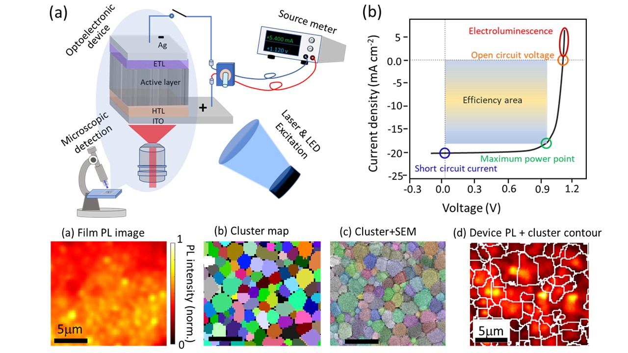
The clusters revealed by CLIM correspond directly to the grain boundaries visible in SEM — but extracted purely from optical fluctuations, non-invasively, and even inside a working solar cell under one-sun illumination.
Beyond CLIM, the line is expanding into super-resolution approaches, deep learning for on-the-fly analysis, and in-operando characterisation of complete devices under electrical bias — bridging the gap between fundamental photophysics and applied device engineering.
Content/clim-concept.jpg.
The core idea is straightforward: pixels within the same perovskite grain share correlated photoluminescence fluctuations (blinking), while pixels in adjacent grains do not. By clustering pixels according to these temporal correlations rather than by intensity alone, CLIM segments the film into its functional building blocks — directly reporting carrier dynamics, recombination, and defect distribution at the grain level.
The approach works on bare films, on complete devices under electrical bias, and across different perovskite compositions and morphologies. It is fully non-invasive and operates with a standard widefield fluorescence microscope.
CLIM — Algorithm Development
Improving and extending the correlation clustering algorithm: automated threshold optimisation, super-resolution extension via SOFI-inspired approaches, and deep learning for on-the-fly analysis at the microscope.
In-Operando Device Imaging
Mapping functional domains in complete perovskite solar cells and LEDs under operational conditions — as a function of applied voltage, current density, and illumination intensity.
Correlative Microscopy
Sequential and simultaneous correlative measurements combining optical (PL, lifetime, Raman) and electron microscopy on the same sample region, to directly connect structure and function.
Self-Healing & Degradation
Imaging the microscopic dynamics of defect formation and healing at perovskite–charge transport layer interfaces under illumination, electrical bias, and thermal cycling.
For the complete record, see my Google Scholar profile.