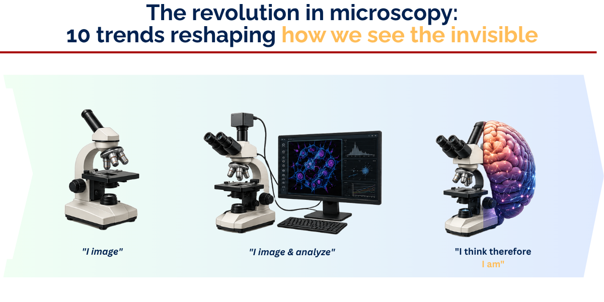
For most of its history, a microscope was fundamentally the same instrument: glass lenses, a light source, and a detector. The resolution limit, set by the wavelength of light, seemed immovable. Super-resolution techniques cracked that barrier two decades ago and earned a Nobel Prize in 2014. But deeper disruptions may still be ahead.
In the past few years, multiple independent threads — computational algorithms, nanophotonic materials, semiconductor fabrication, and artificial intelligence — have converged on optical microscopy at the same time. The result is a field that looks quite different from what it did even five years ago. This article maps ten trends that researchers, engineers, and anyone building tools at the intersection of light and matter should be tracking. It is not an ordered list nor a ranking, just recent trends I’ve observed as I try my best to follow their evolution. Each section includes key recent references and a review or roadmap for anyone who wants to learn more.
1. Computational microscopy
Perhaps the broadest shift underway is the redefinition of what a microscope actually does. Traditionally, a microscope was a hardware problem: better lenses, better detectors, better mechanics. Computational microscopy replaces or supplements the physical optics with algorithms, extracting information that no single lens could capture alone. Consequently, increasingly simple optical setups combined with powerful reconstruction algorithms can match the output of far more complex hardware. Its influence extends well beyond standalone computational imaging systems: autonomous microscopy, label-free super-resolution, photonic chip platforms, and lens-free imaging all depend on computational reconstruction as a core enabling layer. In that sense, computational microscopy is less a single trend and more the infrastructure on which much of the rest of this list is built.
Deconvolution — using knowledge of the microscope’s point spread function to reverse optical blurring — established the principle decades ago and remains widely used in fluorescence imaging today. More recent techniques push this logic further: coherent diffractive imaging (CDI) and ptychography reconstruct full-field, high-resolution images from diffraction patterns rather than direct imaging. A recent comprehensive review in Nature highlighted how these methods now deliver atomic-scale imaging across physical sciences, materials research, and semiconductor inspection. The integration of deep learning has further accelerated the field: physics-informed neural networks can reconstruct images from as few as a single shot, compensate for optical aberrations in real time, quantify phase, and dramatically extend temporal resolution in dynamic imaging scenarios.
Another example is virtual staining, in which a deep learning model is trained to transform label-free, unstained microscopy images into fully colourized, stained sample images. This makes the staining non-invasive and makes it easier to combine multiple stainings at once and/or reuse the sample, since it remains pristine.
Higher-resolution, higher-quality images with on-the-fly processing and adaptive optics — without expensive hardware.
Further reading:
- Physical sciences imaging review — IOP
- Atomic-scale imaging with ptychography — Nature
- Deep learning aberration correction — Applied Physics B
- Physics-informed reconstruction — Nature Methods
- Virtual staining advances — Nature Biotechnology
2. Smart and autonomous microscopy
A microscope that requires a trained operator to make real-time decisions about where to image, when to adjust acquisition, and how to respond to sample dynamics is a significant throughput bottleneck, particularly in clinical and industrial screening contexts. Smart microscopy replaces or augments these decisions with automated, closed-loop control, and the approach has moved well beyond research prototypes into commercial platforms.
In practice, this ranges from relatively modest automation — AI-triggered z-correction, automated focus, or region-of-interest detection — to fully autonomous systems that can detect rare cellular events, switch illumination modes, adjust exposure, and log decisions without human intervention. A recent Nature Methods paper illustrates the maturity this approach is reaching: Daetwyler et al. developed a self-driving, multiresolution light-sheet microscope that simultaneously tracks subcellular dynamics in the context of whole living organisms, automatically following a region of interest as it moves and grows over hours of imaging, switching between low- and high-resolution modes without operator input. Applied to cancer invasion and immune–cancer cell interactions in zebrafish xenografts, the system kept selected regions in focus across multi-hour acquisitions while continuously adapting to sample movement and growth.
The distinction from computational microscopy is worth drawing clearly: computational microscopy is primarily about image formation and reconstruction; smart microscopy is about instrument control and experimental decision-making. In practice, the two are obviously tightly linked; the same AI infrastructure increasingly handles both, and the boundary between “how the image is formed” and “what the microscope does next” will be harder and harder to draw as they both co-evolve.
Continuous, unattended acquisition with adaptive experimental logic, enabling longitudinal experiments and rare-event detection that simply could not be run with human-in-the-loop workflows.
Further reading:
- Smart microscopy review — De Gruyter Brill
- Adaptive imaging methods — Small Methods
- Self-driving light-sheet microscopy — Nature Methods
- Autonomous acquisition — Nature Communications
3. SPAD array detectors
Single-photon avalanche diode (SPAD) arrays are transforming laser scanning microscopy by preserving the full spatial and temporal information encoded in each detection volume — information that conventional single-element detectors discard by integrating all photons into a single intensity value. A SPAD array effectively makes every confocal scan position a small camera, enabling post-acquisition reassignment of photons that was impossible with point detectors.
The most immediate consequence is image scanning microscopy (ISM): a √2 improvement in lateral resolution over conventional confocal, approaching a factor of 2 when combined with deconvolution, with simultaneously improved signal-to-noise, derived entirely from detector architecture and computation rather than changes to the optical path. More broadly, the same photon-resolved dataset simultaneously enables fluorescence lifetime imaging (FLIM), fluorescence correlation spectroscopy, and multi-species discrimination, all from a single acquisition with no hardware modifications. Recent work published in Nature Photonics pushed this further with structured detection (s²ISM), achieving near-isotropic 3D super-resolution by using the spatial arrangement of SPAD pixels to encode angular information during detection rather than requiring structured illumination — a meaningful reduction in light dose and system complexity.
What distinguishes this trend from many others on this list is that the hardware is now commercially available. SPAD array detectors can be integrated into existing confocal microscopes as drop-in upgrades, meaning the capabilities described above are accessible without rebuilding a system from scratch. That combination of multi-modal information from a single acquisition and straightforward retrofittability is what positions SPAD arrays as a genuinely field-wide shift rather than a specialist technique. Recent versions also allow for widefield FLIM imaging, and I would not be surprised if most labs decide to acquire these detectors in the near future.
Rich spatiotemporal photon data from every scan position, turning a standard confocal acquisition into a simultaneous source of super-resolution images, lifetime maps, and molecular dynamics readouts.
Further reading:
- Image scanning microscopy foundations — Optica
- SPAD array applications — Nature Photonics
- Structured detection s²ISM — Nature Photonics
4. Label-free microscopy
Super-resolution has historically depended on fluorescent labels, either for stochastic blinking (SMLM) or for structured illumination contrast. Labels introduce real constraints: they can perturb the sample, photobleach, and cannot always be applied. Multiple independent approaches are now converging on label-free super-resolution, through quite different strategies.
Chip-based platforms exploit the evanescent field of photonic waveguides as an incoherent illumination source, achieving 1.9–2.8× improvement over the diffraction limit on unstained biological samples, including extracellular vesicles and tissue sections. Interferometric image scanning microscopy (iISM), developed by Küppers and Moerner at Stanford, takes a different route, combining interferometric scattering with ISM to image intracellular organelles in live cells at ~120 nm resolution, with no labels, tenfold lower illumination power, and unlimited observation time. iSCAT, in general, has enabled the detection of small particles down to single proteins. A third approach, limited-size object microscopy (LSOM, Nature Photonics), uses prior knowledge about object size alone to surpass the diffraction limit, achieving λ/8 resolution in the far field with no labels and no assumptions about object shape.
The convergence of several independent strategies toward the same goal is a reliable signal that label-free super-resolution is moving from isolated demonstrations toward a genuine methodological frontier.
Nanoscale structural imaging in near-native conditions — without the perturbation, photobleaching, and accessibility constraints of fluorescent labeling.
Further reading:
- Chip-based label-free imaging — Laser & Photonics Reviews
- Label-free imaging methods — Communications Engineering
- Interferometric ISM — Light: Science & Applications
- Limited-size object microscopy — Nature Photonics
- iSCAT single-particle detection — Nature Communications
5. Metasurfaces and flat optics
A conventional microscope objective is a marvel of optical engineering, but also a bulky, expensive, chromatic-aberration-prone component that has changed little in decades. Metasurfaces offer a fundamentally different approach: ultra-thin, nanostructured surfaces that control the phase, amplitude, and polarization of light at sub-wavelength resolution, replacing centimeters of glass with a single structured layer.
Metalenses, the imaging-focused variant, can now match or approach the performance of conventional refractive lenses in specific applications while occupying a fraction of the space and weight. Recent work has demonstrated meta-microlens arrays beginning to replace conventional refractive MLA designs in parallelized confocal systems, improving acquisition speed and reducing photobleaching without requiring hardware redesign. A Nature Communications paper published in early 2026 reported a compact quantitative phase imaging system combining a nanophotonic metasurface with AI-driven aberration correction, achieving sub-micron resolution at 74 frames per second from a single optical layer. Beyond imaging, metasurfaces are enabling new capabilities in polarization multiplexing, wavefront sensing, and computational optics — functions that previously required multiple bulk optical elements.
The transition toward engineering reality is being driven by CMOS-compatible fabrication: the same semiconductor processes used for chip manufacturing can now produce metasurfaces at scale, and the first industrial products have been announced. The remaining challenges — efficiency losses, chromatic dispersion over broad bandwidths, and manufacturing yield — are active research fronts rather than fundamental barriers.
Miniaturised, lightweight optical systems with programmable wavefront control, critical for endoscopy, wearable imaging, and the integration of optics with photonic chips.
Further reading:
- Metasurface imaging systems — Communications Engineering
- Metalens fabrication — ACS Nano
- Flat optics roadmap — Nature Reviews Materials
- Metasurface fundamentals — Science
- Quantitative phase imaging with metasurfaces — Nature Communications
- Metasurface applications in microscopy — Light: Science & Applications
6. Photonic chip / integrated circuit microscopy
One of the more counterintuitive developments in microscopy is that the substrate the sample sits on is becoming part of the optical system. Photonic integrated circuits (PICs) — chips containing optical waveguides fabricated using semiconductor processes — can deliver highly controlled evanescent illumination directly to the sample surface, enabling super-resolution imaging without a conventional objective-based excitation path.
Waveguide-based total internal reflection fluorescence (TIRF) decouples excitation from collection entirely. The chip illuminates; any standard objective collects. This architectural separation enables uniform, wide-field illumination at intensities and confinement lengths that conventional objective-based TIRF cannot easily match, over fields of view that scale with chip area rather than objective NA. Several super-resolution modalities — dSTORM, SIM, SRRF — have now been demonstrated on chip platforms, and companies such as Chip NanoImaging are commercializing the approach for biological and pathology applications. Material development is advancing in parallel: a 2025 paper demonstrated an aluminum oxide waveguide platform with autofluorescence background approximately 200 times lower than silicon nitride at 405 nm, extending the usable spectral range toward the UV.
The advantages come with a drawback: evanescent illumination is confined to within roughly 100–200 nm of the chip surface, making it well-suited for membrane dynamics, extracellular vesicles, and surface-proximal cellular processes, but not for imaging through tissue or at depth. As the technology develops, it is likely that it will broaden its range of applications.
Scalable, high-throughput super-resolution over large fields of view, decoupling illumination quality from objective choice and addressing one of the longstanding bottlenecks of nanoscopy.
Further reading:
- Waveguide-based TIRF — Light: Science & Applications
- Photonic chip material development — Light: Science & Applications
- Chip-based nanoscopy — Nature Photonics
7. Expansion microscopy
Expansion microscopy is not a new technique; the core concept of embedding tissue in a swellable polymer gel and physically enlarging it before imaging was introduced a decade ago. What has changed recently is the scale of expansion and the richness of the information that can be extracted, which together are making the approach newly relevant to questions that previously required electron microscopy.
Early implementations achieved 4× linear expansion, roughly doubling effective resolution over the diffraction limit. Recent advances have pushed this to 16–24×, corresponding to effective resolutions of approximately 15 nm — approaching EM scales on a standard confocal microscope. The pan-ExM-t method demonstrated this on mouse brain tissue with simultaneous pan-staining for ultrastructural context and antibody labeling for molecular specificity, producing what the authors described as CLEM-like (correlative light and electron microscopy) insights without the sample preparation complexity or instrument cost of actual electron microscopy. The combination of near-EM ultrastructural detail and molecular specificity, on hardware most biology labs already own, represents a meaningful shift in what is accessible to structural cell biology.
Recent work on arXiv has reported an expansion factor of x1000, enabling the visualization of protein structure, optically.
Up to EM-scale structural resolution with fluorescence molecular specificity, on existing confocal hardware.
Further reading:
- Expansion microscopy methods — Nature Communications
- Original expansion microscopy — Nature Communications
- Pan-ExM-t method — Nature Biotechnology
- x1000 expansion factor — bioRxiv
8. Democratization: bringing high-performance microscopy out of the core facility
A thread running through several trends on this list — computational reconstruction, chip-based illumination, metasurface optics, open-source instrument control — is the progressive reduction of the cost and expertise threshold for high-performance microscopy.
The clearest technical expression of it is lens-free imaging: placing a sample directly above an image sensor and reconstructing the object computationally from the recorded diffraction pattern. The approach trades optical complexity for algorithmic complexity, and the resulting systems are compact, lightweight, and inexpensive. Techniques including digital holography, Fourier ptychographic microscopy (FPM), and coded ptychography recover both amplitude and phase from intensity-only measurements; FPM has achieved whole-slide imaging throughput exceeding high-end commercial scanners at a fraction of the system cost.
Recently, a smartphone-based super-resolution microscope (Loretan et al.), achieving single-molecule sensitivity and ~80 nm localization precision at a hardware cost below €350, illustrates how far this logic can be pushed when computational power is abundant.
The downstream implications extend well beyond instrumentation. Portable diagnostics, field-deployable pathology in resource-limited settings, classroom-accessible imaging, and scalable environmental monitoring all become tractable when the hardware barrier drops this far. Open-source control software such as Micro-Manager, combined with commodity sensors and 3D-printed optomechanics, is extending the same logic to more conventional microscope architectures. The question is no longer whether high-performance imaging can be made accessible — it demonstrably can — but how quickly the surrounding ecosystem of reagents, validated workflows, and training will follow.
Research-grade imaging in portable, low-cost form factors, extending access to analytical microscopy beyond well-equipped central facilities.
Further reading:
- Lens-free imaging review — Light: Science & Applications
- Fourier ptychographic microscopy — Optics Express
- Micro-Manager open-source control — Nature Methods
- Smartphone-based super-resolution microscopy — Nature Communications
9. Correlative microscopy
Correlative microscopy — combining two or more complementary techniques on the same region of interest — is moving from a specialist workflow to a mainstream practice, driven by improvements in sample registration, automated stage navigation, and integrated instrument platforms. Historically this meant sequential acquisition on separate instruments, with all the sample preparation and registration challenges that entails. Increasingly, purpose-built platforms perform multiple modalities on a single setup, reducing both workflow complexity and the risk of sample perturbation between acquisitions.
In biology, the classic combination is CLEM: correlative light and electron microscopy, which pairs the molecular specificity of fluorescence with the ultrastructural detail of EM. Recent advances have dramatically reduced the friction of this workflow. Expansion microscopy is producing CLEM-like results on standard confocal hardware; the pan-ExM-t method described earlier achieves near-EM ultrastructural resolution with simultaneous antibody labeling, without requiring an electron microscope at all. At the same time, cryo-CLEM workflows are maturing, enabling the same sample to be imaged by fluorescence and then by cryo-electron tomography with minimal perturbation. Nature Methods named EM-based connectomics its Method of the Year for 2025, reflecting how optical and electron modalities are being combined to reconstruct neural circuits at previously inaccessible scales. The convergence with spatial omics is adding a third layer: spatial transcriptomics and proteomics methods now allow the same tissue section to yield morphology, ultrastructure, and genome-scale molecular identity simultaneously.
In materials science the trend is equally active. FIB-SEM combined with Raman spectroscopy, X-ray tomography, or EBSD is becoming a standard characterization stack for battery materials, alloys, and advanced composites, correlating electrochemical performance with structural features at the nanoscale. ZEISS, Thermo Fisher, and Delmic have all announced or shipped commercial correlative workflow platforms, signalling that the field has crossed from research prototype to routine instrumentation.
The underlying driver in both domains is the same: the questions being asked have become too multidimensional for any single technique to answer. Correlative microscopy is the structural response to that complexity.
Simultaneous access to morphology, chemistry, molecular identity, and ultrastructure from the same sample region, replacing sequential single-modality studies with integrated, multidimensional characterization.
Further reading:
- Correlative imaging in neuroscience — Nature Reviews Neuroscience
- Correlative workflows — Nature Cell Biology
- Correlative materials characterization — Chemical Reviews
- FIB-SEM correlative methods — Advanced Materials
- Spatial omics convergence — Nature Biotechnology
10. The emergence of quantum microscopy
Quantum microscopy has been around for a while, but recent papers have shown progress and started to demonstrate real-world potential.
The first is quantum-enhanced sensitivity. By exploiting entangled or correlated photon states, imaging systems can, in principle, surpass the classical shot noise limit — the fundamental sensitivity ceiling of any measurement based on independent photons. He et al. demonstrated quantum microscopy of biological cells at the Heisenberg limit using entangled biphoton sources, achieving sensitivity improvements that would require proportionally higher photon flux to match classically — directly relevant for imaging live, photosensitive samples. The SPAD array detector technology described earlier in this article is a key enabler here: its single-photon sensitivity and timing resolution make it one of the few detector architectures capable of capturing entangled photon correlations at biologically relevant rates.
The second is quantum sensing. Rather than using quantum light to image a sample, this approach uses quantum systems — typically nitrogen-vacancy (NV) centers in diamond — as probes that are exquisitely sensitive to local magnetic, electric, or strain fields. Healey et al. demonstrated this using van der Waals heterostructures as quantum sensors, imaging magnetic properties at the nanoscale with a spatial resolution and field sensitivity that no classical optical technique can approach. This branch of quantum microscopy is arguably closer to practical application than entangled photon imaging, and is already finding use in materials characterization and condensed matter physics.
The practical barriers differ between the two approaches but share a common theme: scalability. Entangled photon sources remain too dim for most biological imaging conditions; NV-center platforms require careful sample integration. Neither barrier is fundamental — both are engineering challenges that the field is actively addressing.
Further reading:
- Quantum microscopy at the Heisenberg limit — Nature Communications
- Entangled photon imaging — Optica
- Quantum sensing fundamentals — Nature Physics
- NV-center quantum sensing — Optica
- Van der Waals quantum sensors — Nature Physics
Where these threads converge
What makes this moment in microscopy unusual is not any single breakthrough but the simultaneity of several independent advances arriving at once. Computational algorithms extract more information from fewer photons. SPAD arrays capture that information with unprecedented temporal and spatial detail. Metasurfaces provide thinner, lighter optics. Photonic chips reimagine the illumination architecture entirely. Smart control systems tie it together, and the same AI infrastructure enabling autonomous acquisition is beginning to remove the label requirement altogether.
These trends do not develop in isolation. Correlative workflows are combining modalities that were previously incompatible. Expansion microscopy is making electron-scale questions answerable on optical hardware. Lens-free and chip-based platforms are moving high-performance imaging out of the core facility and into field and clinical settings.
No single instrument embodies all of these trends yet. But the systems being designed today are beginning to incorporate two or three of them simultaneously, and the resulting performance is qualitatively different from what a conventional microscope can deliver.
The practical question for researchers and engineers is not which trend to follow, but which combination of these capabilities is most relevant to the measurement problem at hand.
Which of these trends do you think is most underrated, and why? I’d be curious to hear from people working closer to any of these areas — and if there’s a trend I missed, I’d like to know that too.