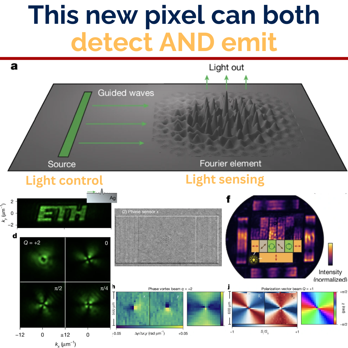
Every camera pixel ever built does one job: it measures how much light hits it. Every display pixel does the opposite job: it emits light of a chosen intensity. Spatial light modulators go a step further and shift the phase of light passing through. But in six decades of pixel design, no single element has controlled amplitude, phase, and polarization together, let alone done that in both directions, sensing incoming light and generating outgoing light from the same structure. A group led by David Norris at ETH Zurich has now closed that gap, packing all of it into a diffractive element just microns across.
Why one pixel doing three things at once matters
Light carries information in three independent channels: how bright it is, what phase it carries, and how it is polarized. Most optical instruments only read or write one of these at a time and rely on a chain of separate components, a polarizer here, a phase plate there, a camera at the end, to handle the rest. That works, but it is bulky, hard to align, and wastes a large share of the light along the way.
Fields like adaptive optics, polarization imaging, and holographic displays all run into this same bottleneck. Correcting a distorted wavefront, for instance, means first sensing its phase and polarization errors and then generating a correction, using two entirely different sets of optics for the two halves of that loop. A single element that can do both would shrink that loop into something close to a real pixel.
How the Fourier pixel works
The approach leans on surface plasmon polaritons, coherent electromagnetic waves that travel along a metal surface. Instead of trying to shape light directly with an array of small resonators, as conventional metasurfaces do, the team routes these plasmons toward a carefully designed wavy microstructure. When the plasmons hit that structure, they scatter into whatever optical wavefront the surface was designed to produce. Run the same device in reverse, and incoming light coupling into the plasmons lets the structure read out the field’s amplitude, phase, and polarization instead of emitting them.
The key departure from standard metasurface design is the interface itself. Metasurfaces approximate a desired wavefront with discrete subwavelength resonators, which becomes numerically difficult once several functions have to be encoded together. Here, the surface profile is a continuous sum of sinusoids, a genuine Fourier surface, so multiple functions can simply be superposed as additional terms rather than re-optimized as a coupled resonator array.
What stands out to me is how simple the design step turns out to be. Because the surface profile only needs to imprint a phase, not solve a full electromagnetic scattering problem, the required height map is just the inverse Fourier transform of the target wavefront, corrected for the momentum mismatch between plasmons and free-space photons. No electromagnetic simulation is involved. The team reports needing roughly a day to go from a concept to a working, fabricated device, largely thanks to a thermal scanning probe lithography process capable of writing that continuous wavy profile with nanometer-scale depth control.
What the devices actually demonstrated
What this unlocks
- Full field control amplitude, phase, and polarization handled together, for both generating and sensing light
- High-order vortex beams Gaussian vortex beams generated with topological charge up to q = +5, verified with a cylindrical-lens interference test
- Single-shot Stokes polarimetry a complete polarization sensor built into one 10 × 10 micron element
- Two material platforms demonstrated in silver for plasmonic devices and in silicon nitride for photonic waveguide modes, opening a path to chip integration
Beyond single-function devices, the group also clustered and superposed several Fourier elements within one pixel to sense amplitude, phase, and polarization simultaneously, arriving at devices with a footprint comparable to a conventional camera pixel. Because the surface profiles are shallow, cross-talk between the superposed functions stays roughly five orders of magnitude below the intended signal, which is what makes stacking multiple functions into one element practical rather than just a nice idea on paper.
Where this could go
The paper points to adaptive optics, holographic and augmented-reality displays, optical communication, and quantum information processing as natural application areas, and it is easy to see why. Any system that currently needs a separate polarizer, phase element, and detector to fully characterize or shape a beam is a candidate for replacement by a single Fourier pixel, or an array of them acting as a combined camera and display.
For anyone working on optical manipulation or structured illumination, the appeal is fairly direct: a single element that maps the amplitude, phase, and polarization of a beam in one shot removes a real source of alignment error and instrumentation bulk from an experimental setup. I would be curious to see this pushed toward dynamic, electrically tunable versions, since the current devices are static once fabricated. Wavelength multiplexing is the other open question worth watching, since a sensor array built from pixels tuned to different colors would start to look like a genuine spectrally resolved polarization camera rather than a single-wavelength demonstration.
What I find most convincing about this work is not just the functionality but the simplicity of getting there. Skipping electromagnetic simulation entirely, and reducing the design problem to an inverse Fourier transform, is the kind of shift that tends to accelerate a field once other groups start building on it.