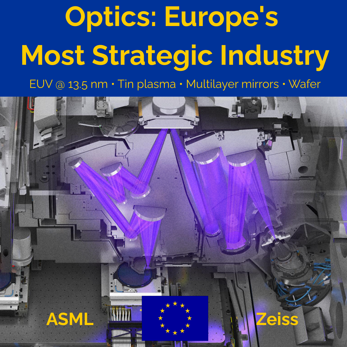
When people ask where Europe stands in the AI race, they usually mean the models — the large language models, the chatbots, the frontier labs. By that measure it is easy to conclude that Europe is a spectator, watching the United States and China trade the lead. But that framing quietly skips a step. AI runs on chips. Chips are printed with light. And the machines that print with light are, to a remarkable degree, European.
I work in optics and imaging, so this is a story I find hard to look away from. The same physics that governs a good microscope — wavelength, numerical aperture, aberration, the stubborn limits of what light can resolve — sits at the heart of the most strategically important manufacturing process on the planet. It is worth understanding, because it changes how you read the geopolitics of technology.
Chips need light, and light needs optics
Every leading-edge processor begins as a pattern projected onto silicon. To shrink transistors, you shrink the features you can print, and the smallest feature you can print is set by the wavelength of the light you use. Modern logic and memory have pushed past the point where ordinary deep-ultraviolet light can keep up. To pattern features at the 5 nm, 3 nm and 2 nm scale, the industry moved to extreme ultraviolet (EUV) light at roughly 13.5 nm — a wavelength so short it is absorbed by air, by glass, by almost everything.
That single constraint reshapes the entire machine.
Because EUV is absorbed by nearly all materials, you cannot use lenses — there is no transmissive glass at 13.5 nm. The whole optical path has to work by reflection, in vacuum, using multilayer mirrors coated to reflect a sliver of that wavelength. Generating the light is just as unforgiving: a high-power laser vaporises tin droplets into a plasma that emits EUV, tens of thousands of times per second.
This is where Europe stops being a spectator and becomes the stage.
The European stack behind every advanced chip
The supply chain for EUV is astonishingly concentrated. A handful of European organisations hold positions that are, in practice, irreplaceable.
- The only company that builds complete EUV lithography systems
- Around 90% share of the lithography-tool market
- High-NA EUV systems priced at roughly $380–400M each
- Sole supplier of the mirrors and optical columns EUV depends on
- Oberkochen and Wetzlar are the only two sites in the world that build them
- ASML's own filings say it could not operate without Zeiss
- High-power CO₂ lasers that vaporise tin to generate EUV plasma
- The drive laser sits at the origin of the whole light path
- imec (BE) runs shared High-NA R&D and early tool qualification
- Jenoptik, SUSS MicroTec and others across masks, DUV and metrology
Europe does not fabricate most of the world’s leading-edge chips — that happens largely in Taiwan and South Korea. But it builds the machines, and the optics inside the machines, without which those chips cannot exist. That is a different, and arguably deeper, kind of leverage.
Why this matters more now than when I first wrote about it
I first sketched this argument in a short post over a year ago. Since then the story has not softened — it has sharpened. EUV has moved from a demanding research technology into the beating heart of the AI hardware ramp, and the numbers have become hard to ignore.
The most significant shift is the arrival of High-NA EUV in real production. In mid-2026, Intel Foundry reported using ASML’s High-NA EUV on its 18A node to build a subset of its Core Ultra “Panther Lake” processors — the first high-volume logic product patterned with the technology. imec, meanwhile, took delivery of the most advanced High-NA system in the world, the EXE:5200, with full qualification expected by the end of 2026.
The scale of the optics is genuinely startling from an instrumentation standpoint. A High-NA projection module contains more than 40,000 parts and weighs around 12 tons — roughly seven times the volume and mass of a standard EUV optic. Individual mirrors are machined for months before they reach the required figure, then coated and polished to tolerances measured in fractions of a nanometre. Zeiss is expanding its Oberkochen complex by about 25,000 square metres to keep up, having grown its semiconductor-optics revenue 23% to just over €5 billion — now the group’s largest business. ASML’s system output is, by its own account, limited by how fast Zeiss can produce these optics.
Optics as geopolitics
None of this has escaped policymakers. Because so much of the leading-edge supply chain runs through a few European doorways, those doorways have become instruments of foreign policy. The United States has repeatedly pressed the Dutch government over export licences for ASML shipments to China — a market that accounted for roughly a third of ASML’s sales in 2025 — and proposed legislation would restrict those sales further.
Europe’s response has been to lean into the idea of technological sovereignty. In June 2026 the European Commission proposed a Chips Act 2.0, part of a wider sovereignty package, that would even grant emergency powers to reprioritise semiconductor production during a shortage. Whether it delivers is another question — it is not yet law — but the framing is telling. The original Chips Act aimed for a 20% share of global chip production by 2030; the newer thinking is more honest about a hard truth: Europe’s real strength is not self-sufficiency but indispensability. It doesn’t need to make everything, if the rest of the world cannot make the most advanced things without it.
The strategic picture, in short
- AI is a hardware story too. Frontier models are downstream of chips, and chips are downstream of light.
- Optics is the chokepoint. EUV lives or dies on ultra-precise European mirrors, lasers, and systems.
- Leverage over autonomy. Europe doesn't dominate fabrication — it controls the tools that make fabrication possible.
For someone who spends their days thinking about how to shape and measure light, there is something quietly satisfying in this. The discipline of optics is often treated as mature, even settled — a solved problem. It is anything but. The ability to bend, focus and pattern light at extreme wavelengths, with unforgiving precision, turns out to be one of the pillars the entire digital economy now rests on. Europe happens to be very good at it. That is not a small thing to be spectating from.
This piece grew out of a short LinkedIn post; the original idea came from a conversation with Dayhana Correa Sánchez and was partly inspired by a video from Freddy Vega. I’ve expanded and updated it with developments through mid-2026.