A chip smaller than a square millimetre just transmitted data at 362 gigabits per second — using light instead of radio waves, and at roughly half the energy cost of a modern Wi-Fi router. This is not a simulation. It is a bench-top experimental result from the University of Cambridge, published in Advanced Photonics Nexus, and it deserves a closer look.
Wi-Fi and cellular networks have carried us remarkably far. But there are real physical walls ahead. Radio spectrum is crowded, particularly in dense indoor environments. Interference compounds as device density increases. And the energy cost per transmitted bit is climbing at a moment when the industry can least afford it — global wireless traffic is projected to exceed 473 exabytes per month by 2030. Something has to give.
Optical wireless communication (OWC) has been proposed as a complementary path forward for more than a decade. The principle is simple: use light instead of radio waves. Light offers orders of magnitude more available bandwidth, cannot penetrate walls (so no inter-room interference), and can be directed with precision. What has been harder is making it practical — fast enough, efficient enough, and manufacturable enough to matter. This paper from Cambridge moves that needle meaningfully.
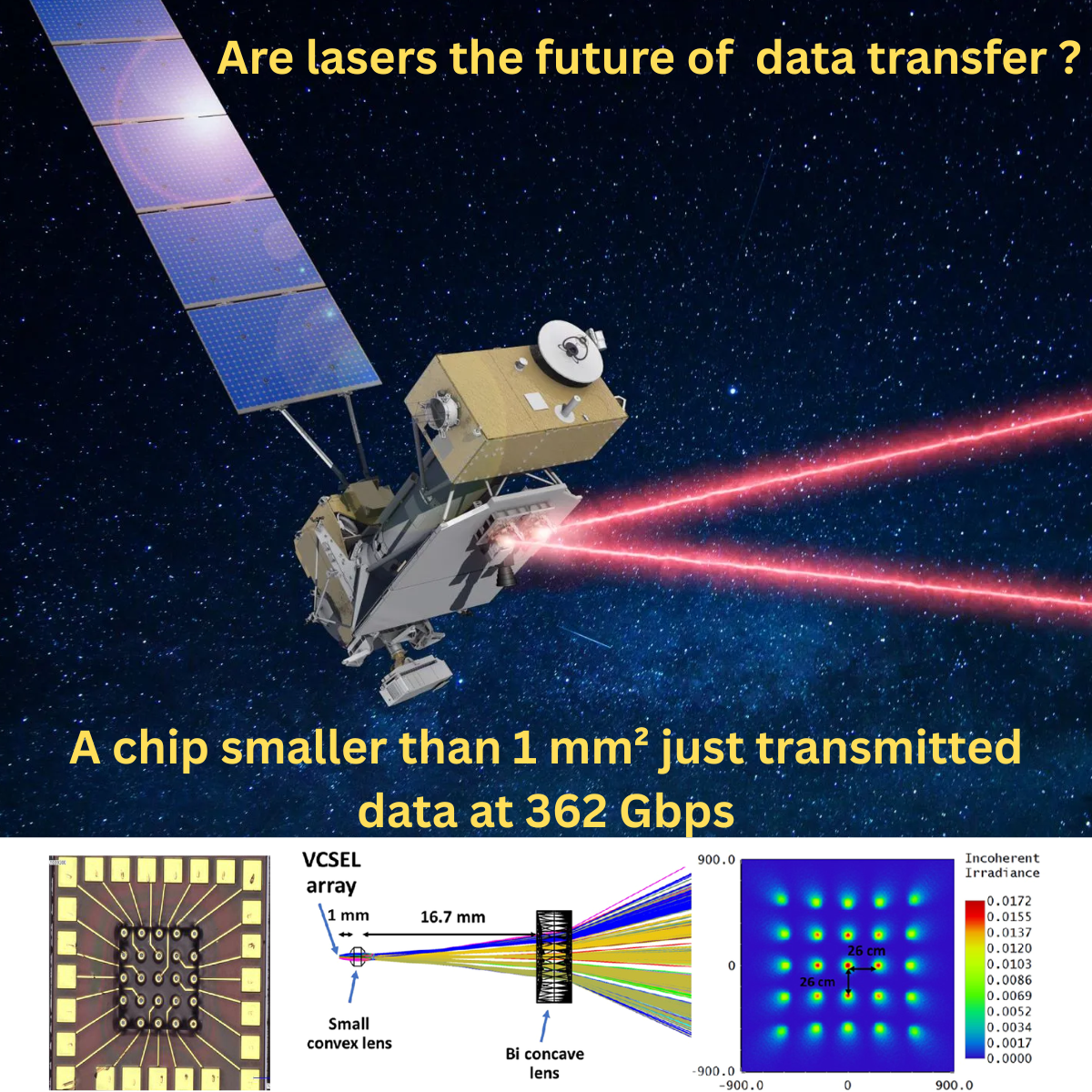
The device: 25 lasers on a chip smaller than a fingernail
At the centre of the system is a custom 5×5 array of vertical-cavity surface-emitting lasers (VCSELs) operating at 940 nm — near-infrared, just beyond visible. VCSELs are a mature technology: they power the Face ID sensor in your phone, the data links inside hyperscaler data centres, and a growing range of sensing and ranging applications. Their appeal here is the same as everywhere else — they are fast, efficient, and can be fabricated in dense arrays on a standard wafer.
The chip measures 845 µm × 810 µm. Each laser has a 15 µm aperture, a threshold current below 2 mA, and an intrinsic modulation bandwidth exceeding 10 GHz. Crucially, each element in the array is independently addressable — each one carries its own data stream, and all streams run in parallel. That is the source of the headline number: the aggregate throughput is the sum across all active channels, not a single link.
Twenty-one lasers, each independently modulated, each carrying between 12.8 and 18.6 Gbps. The total: 362.71 Gbps from a chip you could lose between your fingers.
Modulation: squeezing every bit from the available bandwidth
The team used direct current-biased optical OFDM (DCO-OFDM) with adaptive bit and power loading — the same family of signalling that underpins LTE and Wi-Fi, now applied to a free-space infrared link. The logic is the same as in radio: split the channel into many narrow subcarriers, measure the signal-to-noise ratio on each independently, and allocate modulation order (here up to 1024-QAM, i.e., 10 bits per symbol) according to what each subcarrier can support. This maximises spectral efficiency without pushing the system into instability.
One constraint is worth noting honestly: the receiver was a commercial off-the-shelf silicon PIN photodiode with a 3 dB bandwidth of 1.4 GHz. The VCSELs themselves support 15 GHz. The system was detector-limited, not source-limited. With a matched receiver, the same chip could plausibly push much further — and that headroom is part of what makes this result interesting.
Beam shaping: from 25 laser spots to a structured illumination grid
Running 25 lasers in parallel creates an obvious problem: without control, the beams diverge and overlap, defeating the purpose of spatial multiplexing. The Cambridge team addressed this with a three-stage custom optical assembly.
Stage 1 — Collimation. A microlens array with a 70 µm pitch — precisely matched to the VCSEL array pitch — sits directly above the chip and collimates each beam individually, suppressing divergence and preventing adjacent beams from merging at short range.
Stage 2 — Separation. A cascade of plano-concave lenses increases the angular separation between adjacent beams, spreading them into a structured grid at the target plane.
Stage 3 — Homogenisation. A pair of beam homogeniser microlens arrays reshapes the native (and non-uniform, donut-like) VCSEL output into clean square spots with flat-top intensity profiles. The result at 2 m distance: a 5×5 grid of square illumination patches with spatial uniformity exceeding 90% across the field.
Homogenisation does carry a cost — redistributing power over a larger area reduces peak intensity, and the paper reports an SNR reduction of up to 5 dB in the shaped-beam configuration. The shaped system still sustained data rates above 11 Gbps per channel, confirming the viability of the trade-off for multiuser applications where coverage uniformity matters more than peak single-link throughput.
Energy efficiency: the underappreciated headline
The 362 Gbps number will attract attention. But the energy story is arguably more important for long-term relevance.
| System | Energy per bit | Notes |
|---|---|---|
| This work (VCSEL array) | ~1.4 nJ/bit | Best and worst channel both ~1.4 nJ/bit |
| State-of-the-art Wi-Fi (802.11ax/ac) | ~2.6 nJ/bit | Under comparable high-throughput conditions |
The VCSEL system consumes roughly 1.8–1.9× less energy per bit than a modern Wi-Fi access point under equivalent loading. For a technology targeting the same indoor connectivity space, that is not a marginal improvement — it is a structural advantage rooted in the physics of direct laser modulation, which requires no upconversion circuitry, no power amplifier chain, and no frequency synthesiser.
The multiuser demonstration
Single-link records are useful benchmarks. What makes or breaks an access technology is its behaviour under simultaneous multiuser load. The team demonstrated this directly: four VCSEL channels activated concurrently, beams spatially separated at the receiver plane by a compact custom lens, four independent photodetectors collecting each channel. The result was an aggregate throughput of approximately 22 Gbps across four simultaneous links, with no prohibitive cross-channel interference. It is a proof of concept for the architecture — and the receiver bandwidth limit applies here too.
Where this fits in the larger picture
A few weeks before this paper appeared, NVIDIA announced a $4 billion investment into laser companies, motivated by the need to replace copper interconnects inside data centres. That story is about photons replacing electrons over the last metre inside a rack. This Cambridge paper is about photons replacing radio waves over the last ten metres between ceiling-mounted access point and user device. The underlying physics is similar — coherent sources, free-space propagation, careful beam management — but the use case and the engineering constraints are different.
The point is not that optical wireless will replace Wi-Fi. Line-of-sight requirements, mobility constraints, and link blocking by physical obstructions all remain real challenges for any free-space optical system. The point is that in controlled indoor environments — offices, hospitals, clean rooms, data centre floors, dense AR/VR deployments — optical wireless offers a complementary channel that radio simply cannot match on bandwidth density and interference isolation. And this paper demonstrates that the transmitter hardware for such a system can be chip-scale, manufacturable, and twice as efficient as the radio alternative.
The future of indoor connectivity is probably not radio alone. It might be radio and light — each doing what it does best.
Congratulations to Hossein Safi, Iman Tavakkolnia, Harald Haas, and the full team at the LiFi Research and Development Centre, University of Cambridge. This work was funded under Project REASON (Future Open Networks Research Challenge, UK DSIT) and published in Advanced Photonics Nexus (SPIE, March/April 2026, Vol. 5(2), DOI: 10.1117/1.APN.5.2.026018).
Frequently Asked Questions
What is optical wireless communication (OWC)?
Optical wireless communication transmits data using light instead of radio waves. It offers vastly more bandwidth, no electromagnetic interference, and inherent directional security. LiFi is the best-known form: a bidirectional, high-speed indoor wireless system operating in the visible or near-infrared spectrum. The IEEE 802.11bb standard, ratified in 2023, marks OWC's formal entry into the Wi-Fi ecosystem.
What is a VCSEL and why is it used in wireless communication?
A VCSEL (vertical-cavity surface-emitting laser) is a semiconductor laser that emits light perpendicular to the chip surface. VCSELs have high modulation bandwidths (often exceeding 10 GHz), excellent energy efficiency, and can be manufactured in two-dimensional arrays on a standard wafer — making them ideal for high-speed, scalable optical wireless transmitters. You likely use them already: the Face ID sensor in modern iPhones relies on a VCSEL array.
Will optical wireless replace Wi-Fi?
Unlikely in the near term — but that is not the right question. Optical wireless is best positioned as a complement to radio: it excels in controlled indoor environments where high throughput, low interference, and energy efficiency matter. Radio handles mobility and non-line-of-sight scenarios better. The two technologies will coexist, with optical wireless progressively taking on the high-density, high-bandwidth segments of the indoor connectivity market.